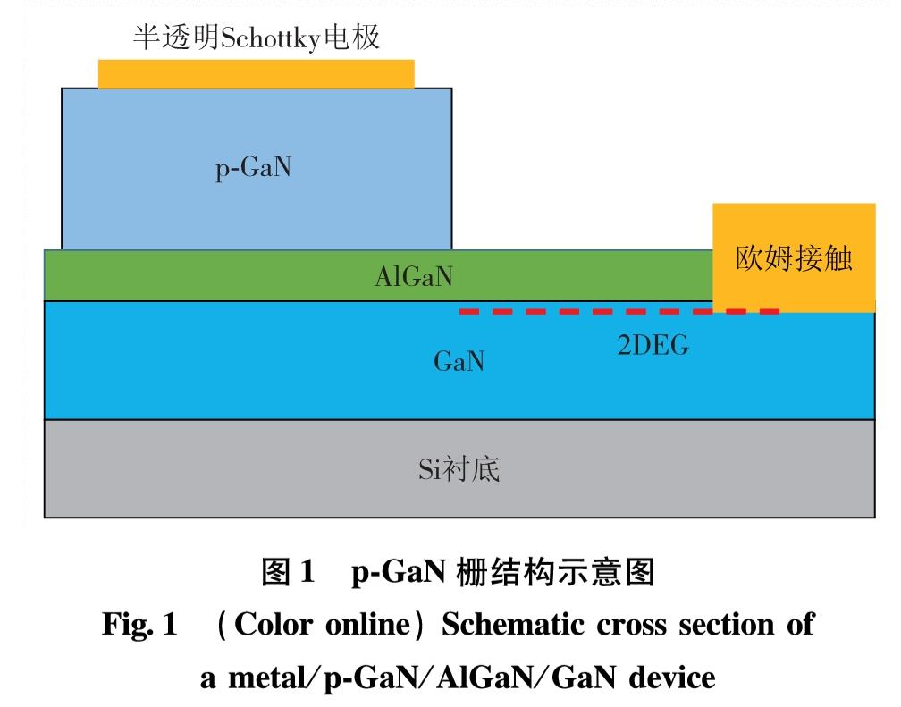
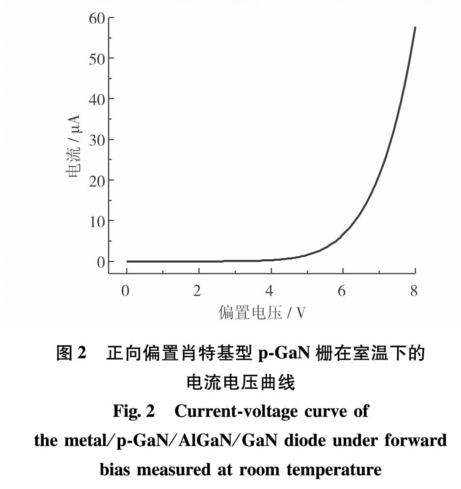
在正向栅压下,p-GaN栅结构中的PIN结,即p-GaN/AlGaN/GaN(2DEG)为正向偏置. 电子可以由2DEG沟道越过AlGaN势垒层注入到p-GaN层. 而p-GaN栅结构中的肖特基结,即金属/p-GaN结为反向偏置. 尽管该肖特基结的势垒高度大于1 eV,但p-GaN上的肖特基结一般具有较大的反向漏电[15-16],在较大偏压下,该肖特基界面也存在空穴注入. 图2为肖特基型p-GaN栅结构的电流电压曲线.
图2 正向偏置肖特基型p-GaN栅在室温下的电流电压曲线
Fig.2 Current-voltage curve of the metal/p-GaN/AlGaN/GaN diode under forward bias measured at room temperature
GaN为直接带隙半导体,电子空穴双向注入时,将发生电致发光. GaN的发光特征与掺杂情况密切相关[17]. Mg掺杂的p-GaN发光谱主要为峰值在 2.8 eV的蓝光峰和在1.8 eV的红光,其中,红光的光强相对较弱. 非有意掺杂的GaN发光谱包括峰值在3.4 eV的带边峰和峰值在2.2 eV的黄光峰. 低激发功率或低注入电流时,低光子能量的发光峰占主导. 随着激发功率或注入电流的增加,高光子能量发光峰的强度增加[17]. 因此,通过不同偏压下的电致发光光谱,可以分析电子和空穴的注入过程.
图3 室温下肖特基型p-GaN栅极在不同正向栅压的电致发光光谱
Fig.3 (Color online)Electroluminescence spectra of a metal/p-GaN/AlGaN/GaN diode under different forward bias voltages measured at room temperature
图3为室温下肖特基金属/p-GaN/AlGaN/GaN器件在不同偏压的电致发光光谱.可见,在4.5 V的偏置电压下,电致发光谱中仅有峰值在1.8 eV的红光峰,表明电子首先由2DEG沟道注入到了p-GaN层. 在p-GaN层中,电子弛豫到深施主能级,空穴弛豫到深受主能级,然后复合发出红光. 当偏置电压大于5 V时,电致发光光谱中出现了峰值在2.2 eV的黄光峰,表明空穴由p-GaN层中被注入到沟道层. 在非有意掺杂的沟道层中,空穴首先弛豫到深受主能级,然后与沟道电子复合发出黄光. 当偏置电压继续增加时,更多电子被注入到p-GaN中,随着深施主-深受主复合中心饱和,导带电子和深受主能级上的空穴复合,发出峰值在2.8 eV的蓝光; 更多的空穴被注入到沟道层,随着深施主能级的饱和,空穴和电子发生带边复合,发射GaN带边3.4 eV的紫外光. 随着偏置电压的进一步增加,3.4 eV的带边发光强度继续增强. 电致发光光谱中的强度震荡来自电致发光在样品上表面和下面反射所导致的干涉现象.
电致发光光谱揭示了p-GaN栅结构在正向栅压下的电子和空穴注入顺序,这有助于研究p-GaN栅HEMT的阈值电压漂移机制. 当“开”态栅压较低时,电子被注入到p-GaN,有可能被电子陷阱俘获,从而导致阈值电压正向漂移. 而当“开”态栅压大于6 V时,大量空穴被注入到沟道层并与2DEG电子复合发射带边紫外光. 高光子能量的紫外光可以激发电子陷阱,抑制阈值电压漂移. 同时,这些高能量光子也可以激发沟道层或缓冲层中的扩展缺陷中心,产生持续光电导效应,从而导致“关”态的漏电增加,影响器件的可靠性.