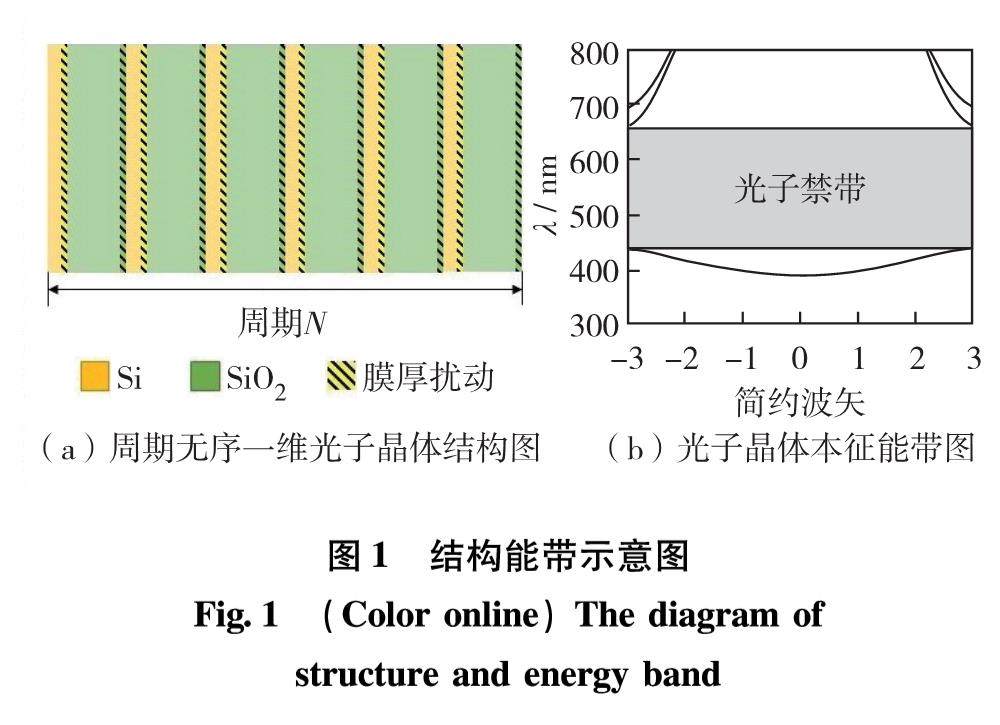
2.1 周期数对光学性质的影响
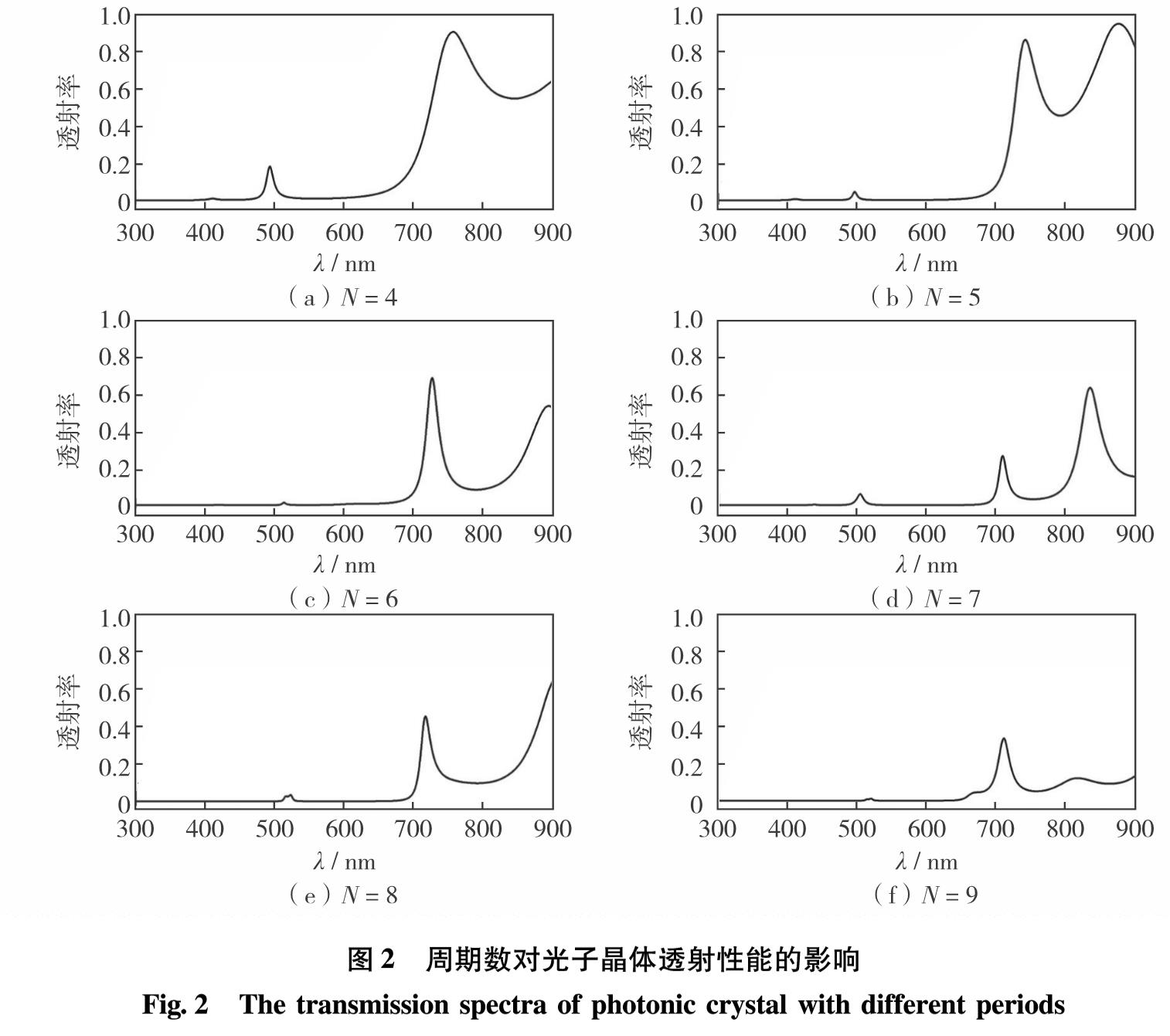
通过比较不同σ的高斯分布分析相应的透射谱.模拟在σ=0.20a时,不同周期数对透射性能的影响,结果如图2.
由于Si材料的吸收,450 nm以下为吸收禁带,图2(a)的光子禁带位于500~670 nm.由于模拟中采取随机误差,禁带位置会在本征能带附近随机偏移.随着层数的增加,整个膜层的无序性增加,薄膜系统变得复杂.随着误差变大,透射率发生复杂波动.禁带宽度变得不稳定,但总体趋于变窄.当层数较大时,某一层的微小误差也会导致整个系统光学性能的改变.另一方面,如果材料的吸收系数不为0,系统的透光率将随着层数的增加而降低.因此,制备光子晶体时应根据精度要求选择合适的周期数.
图2 周期数对光子晶体透射性能的影响
Fig.2 The transmission spectra of photonic crystal with different periods
2.2 两种材料对光学性质的影响对比
本研究选取N=6, 研究随机误差在-0.2a~0.2a时,光子晶体禁带宽度及透过率随Si及SiO2层的厚度变化的变化情况,结果如图3.
图3 两种薄膜膜厚误差不同时,禁带位置的变化
Fig.3 (Color online)Variation of band gap position with different thickness errors of two kinds of film
由图3可见,随着Si层厚度的增加,光子禁带由446~670 nm红移至572~853 nm,禁带宽度由224 nm增至281 nm,增加了25.45%.当SiO2层厚度增加时,光子禁带由446~670 nm红移至476~765 nm,禁带宽度由224 nm增至289 nm,增大了29.02%.对比图3(a)和(b)可见,光子晶体的禁带位置对Si层厚度的变化较为敏感.这是由于Si的折射率较大,当物理厚度变化相同时,Si的光学厚度改变更大,导致禁带漂移较大.当禁带红移量大于50 nm时,光子禁带与该膜层的吸收禁带重合,形成超宽禁带的带阻滤波.对于光子晶体层数较少的简单系统,薄膜厚度误差对系统光透射率的影响较小,禁带位置会发生漂移,并与误差成线性关系.禁带宽度则对SiO2层较为敏感.
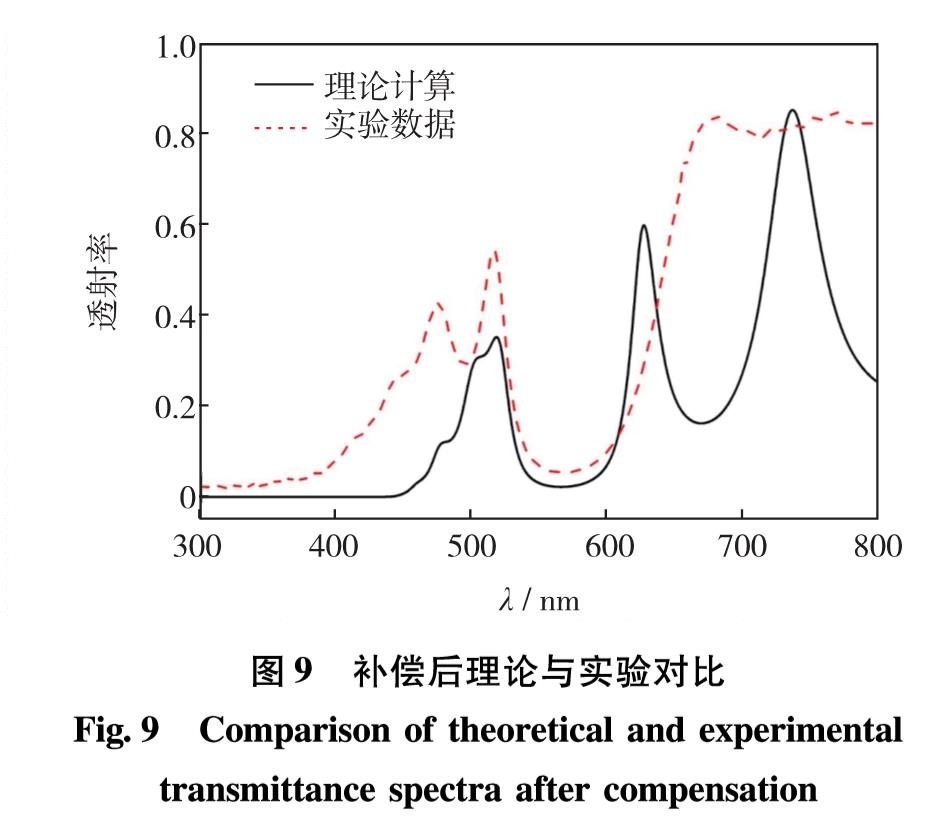
根据理论设计的(Si/SiO2)N结构模型,本研究采用型号为JGP- 450B的磁控溅射镀膜仪实验制备光子晶体多层膜样品.基底采用2 cm×2 cm的高纯石英玻璃,靶材采用纯度为5N的Si和SiO2,本底真空度为4.0×10⁻⁴ Pa,采用型号为STM-2XM的膜厚仪控制膜层的厚度.选定N=6,在高纯石英玻璃基底上交替镀Si和SiO2薄膜.采用功率为40 W的射频磁控溅射制备Si,采用功率为60 W的射频磁控溅射制备SiO2.制备的光子晶体样品利用R1角分辨率光谱仪测量其透射谱.
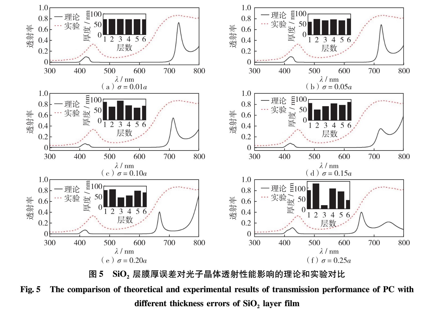
理论模拟不同膜厚随机波动幅度的光子晶体透射性能.对于a=110 nm的光子晶体结构,选取σ分别为0.01a、 0.05a、 0.10a、 0.15a、 0.20a及0.25a的随机膜厚误差,并分别对Si和SiO2层进行讨论.将模拟数据与光子晶体实验样品的测量透射谱进行对比.图4为实验和理论光子晶体透射对比图.其中,SiO2层保持dSiO2=0.66a不变,仅改变每层Si的厚度.
从图4可见,存在厚度扰动的光透过率曲线与设计值相差较大,其原因在于光子晶体多层膜系的每一层均存在误差,因此,整个系统的光学相位就会因误差累计而发生变化.层数越少,累计的光学相位误差越小,误差对光透射性质的影响也就较小.由于设计的误差值为随机误差,禁带位置会在能带附近随机摇摆.图5为保持Si层的dSi=0.34a不变,仅改变每层SiO2的厚度时,膜厚误差对禁带宽度的影响.相比于Si层的厚度误差,SiO2层的误差对透光率的影响较小.这是由于SiO2作为低折射率材料,膜厚误差所引起的光学误差较小.
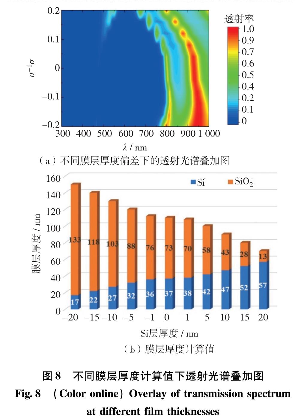
图6对比两种材料误差对禁带宽度的影响.当Si层扰动σ=0.01a时,禁带宽度为本征能带的111.16%; 当Si层扰动σ=0.25a时,禁带宽度仅为37.67%.当SiO2层扰动σ=0.01a时,禁带宽度为本征能带的111.56%; 当SiO2层扰动σ=0.25a时,禁带宽度为76.83%.可见,Si的误差值对光子晶体的禁带宽度影响较大,说明光子晶体的禁带宽度对折射率较大材料的膜厚变化较为敏感.由于膜厚偏差为随机误差,禁带宽度的偏移不是线性的.但总体趋势呈线性关系,而且会越来越趋近于光子晶体材料的本征光子能带.光子晶体本征能带宽度为224 nm,而当厚度偏差σ<0.10a时,禁带宽度超过了本征能带宽度.这是因为引入了膜厚的高斯扰动,相当于将不同频域的光子晶体进行禁带叠加.当随机偏差较小时,会使禁带宽度略微拓宽.